
ASIC Design
Architecture development, front-end design and back-end implementation — a complete RTL-to-GDSII capability delivered by engineers with multiple tape-outs on advanced nodes.
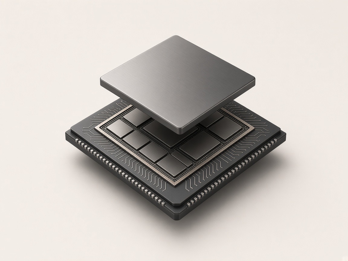
Architecture Development
Our architects understand your product requirements and define the right architecture for your SoC. We analyse the IPs that can become part of your design, recommend the most appropriate technology node, and evaluate chiplet-based partitioning where it better serves your Power, Performance and Area (PPA) targets.
Requirements to specification
Use-case analysis, performance modelling and feature partitioning.
IP & node selection
Make/buy analysis, third-party IP evaluation and process-node trade-offs.
PPA estimation
Early area, power and timing budgets to de-risk the schedule.
Chiplet architecture
Die-to-die interface and partitioning strategies for multi-die systems.
Front-end RTL Design
Our RTL team is proficient in defining SoC architecture and micro-architecture for IPs and subsystems. We develop IPs from scratch and ensure they are IP-XACT compliant; for subsystems and SoCs we integrate in-house and third-party IPs and bring up the full design. Every deliverable is Lint-, CDC- and low-power-clean and ready for synthesis and DFT.
What we deliver
- Micro-architecture specifications and interface documents
- Synthesizable SystemVerilog / Verilog / VHDL RTL
- SoC integration: interconnect, memory map, clock & reset trees
- Lint, CDC and RDC clean reports with waivers documented
- UPF power intent and low-power static checks
- Design reviews, documentation and hand-off to DV / DFT / PD
Synthesis & Static Timing Analysis
We develop and validate timing constraints for functional and test modes, run logic synthesis with PPA optimisation, and lead multi-corner, multi-mode static timing analysis through signoff — including SI, OCV/AOCV/POCV and IR-aware timing.
SDC development
Clocks, exceptions, IO constraints and constraint validation.
Logic synthesis
Physical-aware, DFT-aware and low-power synthesis with UPF.
Formal equivalence
RTL-to-gate and gate-to-gate LEC at every netlist hand-off.
Signoff STA
MCMM closure, ECO generation and hierarchical timing models.
Back-end Physical Design
Our team excels in physical design, static timing analysis and physical verification. Our implementation methodology in floorplanning, placement and clock tree synthesis enables us to time-close even very high-speed designs in a predictable manner — meeting tight tape-out timelines with first-pass silicon-ready results.
What we deliver
- Floorplanning, power planning and macro placement
- Placement, CTS and routing on advanced FinFET nodes
- Timing, IR/EM and signal-integrity closure
- Physical verification: DRC, LVS, antenna and DFM
- Hierarchical and top-level integration
- ECO implementation and tape-out checklists
Tools & Methodologies
We work in your environment with the industry-standard EDA flows your teams already trust.
We're hiring ASIC designers
ASIC Design Engineer · RTL / Digital Design Engineer · Physical Design Engineer · Lead ASIC Physical Design Engineer · Synthesis & STA Engineer